Introduction
The semiconductor industry relies on sophisticated technologies at every stage—from initial chip design to final manufacturing. Two acronyms frequently appear in industry discussions: EDA (Electronic Design Automation) and SECS/GEM (SEMI Equipment Communications Standard/Generic Equipment Model). While both are essential to semiconductor operations, they serve fundamentally different purposes and operate at completely different stages of the production lifecycle.
Understanding the distinction between EDA and SECS/GEM isn’t just academic—it’s critical for professionals working across the semiconductor value chain, from design engineers to fab operators. This comparison explores what each technology does, where it fits in the semiconductor workflow, and why both remain indispensable despite their different roles.
What Is EDA?
Electronic Design Automation (EDA) refers to software tools used to design electronic systems, particularly integrated circuits and printed circuit boards. EDA tools enable engineers to design, simulate, verify, and optimize complex semiconductor devices before any physical manufacturing occurs.
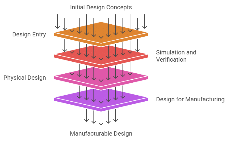
The EDA process encompasses several critical functions:
Design Entry: Engineers use schematic capture tools or hardware description languages (HDL) like Verilog and VHDL to describe circuit functionality. These tools allow designers to work at high abstraction levels, defining what a chip should do rather than manually placing every transistor.
Simulation and Verification: Before committing to expensive manufacturing, designers simulate circuit behavior under various conditions. Functional simulation verifies logical correctness, while timing simulation ensures the design meets performance requirements. Verification tools check that designs match specifications and don’t contain errors that could cause manufacturing failures.
Physical Design: Once verified, placement and routing tools determine where components sit on the chip and how connections between them are formed. This stage considers manufacturing constraints, heat dissipation, signal integrity, and power consumption.
Design for Manufacturing (DFM): Modern EDA tools analyze designs for manufacturability, identifying potential problems that could reduce yields or cause manufacturing failures. They ensure designs comply with foundry process rules and optimize layouts for better production outcomes.
Major EDA vendors include Synopsys, Cadence Design Systems, and Siemens EDA (formerly Mentor Graphics). These companies provide comprehensive tool suites covering the entire design process from concept to tape-out—the point where designs are ready for fabrication.
What Is SECS/GEM?
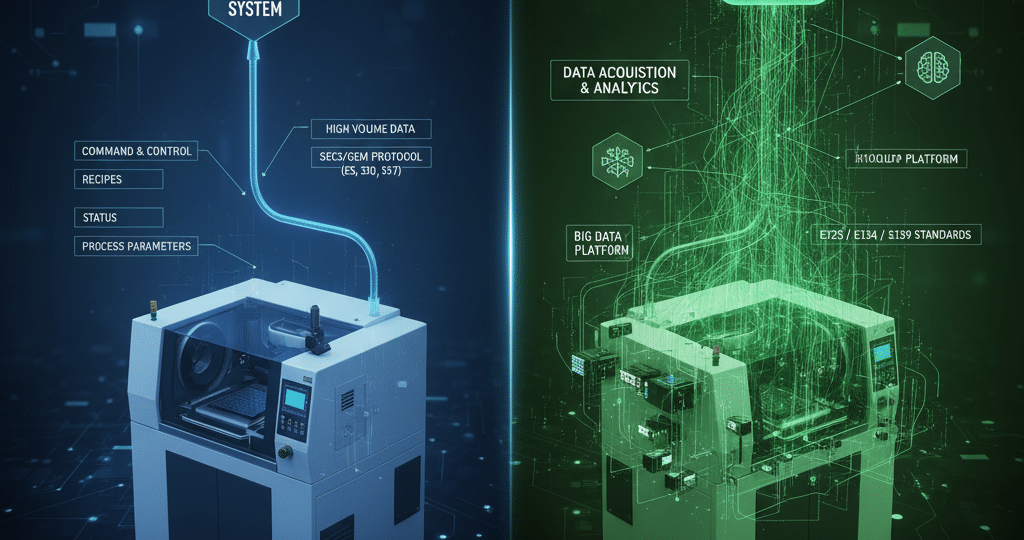
SECS/GEM operates in a completely different domain: manufacturing execution and equipment communication. While EDA focuses on designing chips, SECS/GEM enables communication between manufacturing equipment and factory automation systems during actual production.
SECS (SEMI Equipment Communications Standard) defines the message format and transport protocol for equipment communication. GEM (Generic Equipment Model) specifies the behavioral model—what states equipment can be in, what events it reports, and how it responds to commands.
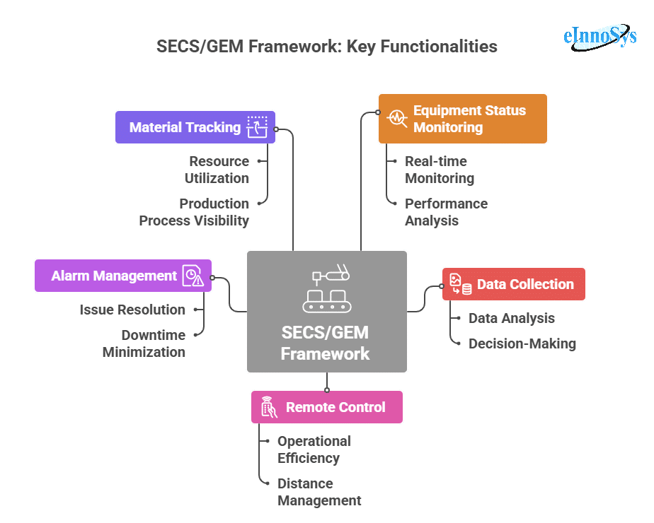
The SECS/GEM framework enables several critical manufacturing functions:
Equipment Status Monitoring: Factory systems receive real-time updates on equipment states—idle, processing, maintenance, or alarmed. This visibility allows operators to manage production flow and respond quickly to issues.
Data Collection: Equipment reports process parameters, measurement results, and production data to Manufacturing Execution Systems (MES). This data drives quality control, yield analysis, and process optimization.
Remote Control: Host systems can send commands to equipment—loading recipes, starting processes, changing parameters—enabling automated factory operations.
Alarm Management: When equipment detects problems, it generates alarms that notify operators and factory systems. Quick alarm response prevents minor issues from becoming major disruptions.
Material Tracking: SECS/GEM supports tracking wafers and other materials through the manufacturing process, ensuring traceability and preventing mix-ups.
Unlike EDA, which involves software engineers and chip designers, SECS/GEM involves automation engineers, equipment manufacturers, and fab operations teams implementing and maintaining communication between hundreds of manufacturing tools and factory systems.
Key Differences Between EDA and SECS/GEM
Lifecycle Stage
EDA operates during the design phase, before manufacturing begins. Engineers use EDA tools to create chip designs that foundries will later manufacture.
SECS/GEM operates during manufacturing. It’s the communication backbone enabling factories to run production equipment efficiently.
EDA serves chip designers, verification engineers, and physical design specialists working for fabless semiconductor companies, integrated device manufacturers, and design service firms.
SECS/GEM serves equipment manufacturers (OEMs) building semiconductor tools, fab automation teams integrating equipment into production lines, and process engineers optimizing manufacturing operations.
Objective
EDA aims to create functional, manufacturable chip designs that meet performance, power, and cost targets while minimizing design time and reducing errors.
SECS/GEM aims to enable seamless communication between equipment and factory systems, supporting automated operations, data collection, and efficient production management.
Why Both Matter
Despite their differences, EDA and SECS/GEM represent complementary aspects of semiconductor production. Effective chip designs created with EDA tools must be manufactured efficiently using equipment that communicates via SECS/GEM. Neither technology can substitute for the other—they operate in different domains addressing different challenges.
Modern semiconductor manufacturing increasingly connects these domains through Design for Manufacturing (DFM) feedback loops. Manufacturing data collected via SECS/GEM informs design decisions made with EDA tools. Yield information, defect patterns, and process variations observed in fabs flow back to designers, allowing them to optimize future designs for better manufacturability.
Conclusion
EDA and SECS/GEM serve distinct, non-overlapping roles in semiconductor operations. EDA enables engineers to design complex chips efficiently, while SECS/GEM enables factories to manufacture those chips efficiently. Understanding both technologies—and how they complement each other—provides essential context for anyone working in the semiconductor industry.
For organizations building semiconductor capabilities, investments in both domains prove necessary. Design excellence enabled by EDA must be matched with manufacturing excellence enabled by robust equipment communication and factory automation. The most successful semiconductor companies excel at both, recognizing that great designs require great manufacturing, and vice versa.
FAQs
-
What is the main difference between EDA and SECS/GEM?
EDA (Electronic Design Automation) is used in the chip design phase to create, simulate, and verify semiconductor designs before manufacturing.
SECS/GEM, on the other hand, is used during the manufacturing phase for equipment communication, automation, data collection, and factory integration.
-
Are EDA and SECS/GEM used in the same part of the semiconductor process?
No. EDA is used early in the lifecycle, during chip design and verification.
SECS/GEM is used later in the fab, enabling real-time communication between manufacturing tools and MES systems.
-
Who uses EDA tools and SECS/GEM systems?
EDA tools are used by chip designers, verification engineers, and layout engineers in fabless companies or IDMs.
SECS/GEM is used by OEMs, automation engineers, integration teams, and fab operations staff responsible for equipment connectivity and production control. -
Why is SECS/GEM important for semiconductor manufacturing?
SECS/GEM ensures standardized communication between equipment and factory systems. It supports recipe control, alarms, data collection, equipment states, and remote command execution—critical for automated fab operations.
-
Why is EDA essential in chip design?
EDA tools help engineers simulate, verify, and optimize complex chip architectures before fabrication. This reduces errors, improves performance, and avoids costly silicon failures during manufacturing.
📅 Posted by Nirav Thakkar on November 18, 2025
Nirav Thakkar
Semiconductor Fab Automation & Equipment Software specialist with 18 years of industry experience.