Photolithography is one of the most critical processes in integrated circuit (IC) manufacturing. It records a binary image on a photosensitive material layer applied to a semiconductor wafer. Precision and efficiency in this stage directly influence wafer yield and overall production quality in advanced semiconductor fabs.
To ensure consistent high yields for memory and logic devices, semiconductor fabs increasingly rely on data monitoring, analysis, and automation. Among these, Fault Detection and Classification (FDC) and recipe automation play a pivotal role in optimizing lithography processes.
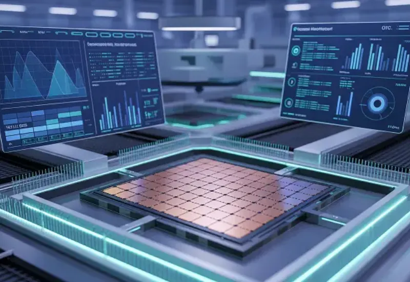
The Importance of Real-Time Monitoring in Lithography
Traditionally, fabs sampled wafers periodically within the production sequence or used test wafers to identify defects. However, this method often delayed problem detection and introduced unnecessary costs.
Today, OEMs integrate sensors and monitors directly into process tools, reducing sampling intervals and improving real-time detection. These inline monitors emulate on-wafer measurements, enabling fabs to interpret tool sensor data quickly and apply corrective measures.
This approach powers fab-wide Fault Detection and Classification (FDC) systems, which:
- Collect real-time equipment data
- Compare results with “Golden” benchmark data
- Trigger automatic responses to prevent defective wafer processing
With automation, fabs no longer need to rely solely on physical inspections, saving significant time and improving troubleshooting accuracy.
How FDC Boosts Yield and Efficiency
By leveraging FDC, fabs can:
- Detect deviations early and stop wafer processing when poor quality is identified
- Reduce corrective action time by eliminating guesswork
- Lower costs by minimizing rework and scrap
- Improve yield and cycle time with precise corrective measures
Einnosys provides a flexible FDC software system tailored to semiconductor fabs’ needs. This system seamlessly integrates with diverse lithography tools and ensures fabs stay competitive with advanced process control. Learn more here
Enhancing Lithography with Metrology and Feedback Loops
Metrology equipment provides vital feedback on overlays and critical dimensions. When integrated with lithography tools, this data helps fabs:
- Auto-analyze overlay data
- Feed corrections back into steppers
- Save significant engineering time
- Improve wafer yield and throughput
This closed-loop automation ensures consistent quality while minimizing manual intervention.
I am text block. Click edit button to change this text. Lorem ipsum dolor sit amet, consectetur adipiscing elit. Ut elit tellus, luctus nec ullamcorper mattis, pulvinar dapibus leo.
Experience Across Global Lithography Tools
Einnosys brings decades of expertise across multiple lithography equipment, including:
- Steppers – Canon, ASML, Nikon
- Tracks – TEL, SVG, DNS
- Metrology tools – KLA-Tencor, Rudolph, Inspectrology
This extensive experience allows Einnosys to design and deploy automation solutions that work seamlessly with diverse fab ecosystems.
Recipe Management and Stepper Job Automation
Another key challenge in lithography is manual job creation, which can lead to errors and inefficiencies. By automating stepper job creation directly from CAD data, fabs eliminate human error and accelerate job setup.
Einnosys’ Recipe Management System (EIRMS) integrates with CAD systems to generate stepper jobs automatically and transfers them to lithography equipment—similar to a JobServer approach. This automation improves accuracy, reduces cycle time, and ensures consistency across production lines. – more here
Lithography remains the backbone of semiconductor manufacturing, and fabs that adopt automation, FDC, and recipe management solutions can achieve significant gains in efficiency, yield, and cost-effectiveness. With its proven expertise and innovative solutions, Einnosys helps fabs worldwide stay ahead in the race for smarter, more productive semiconductor manufacturing.


