
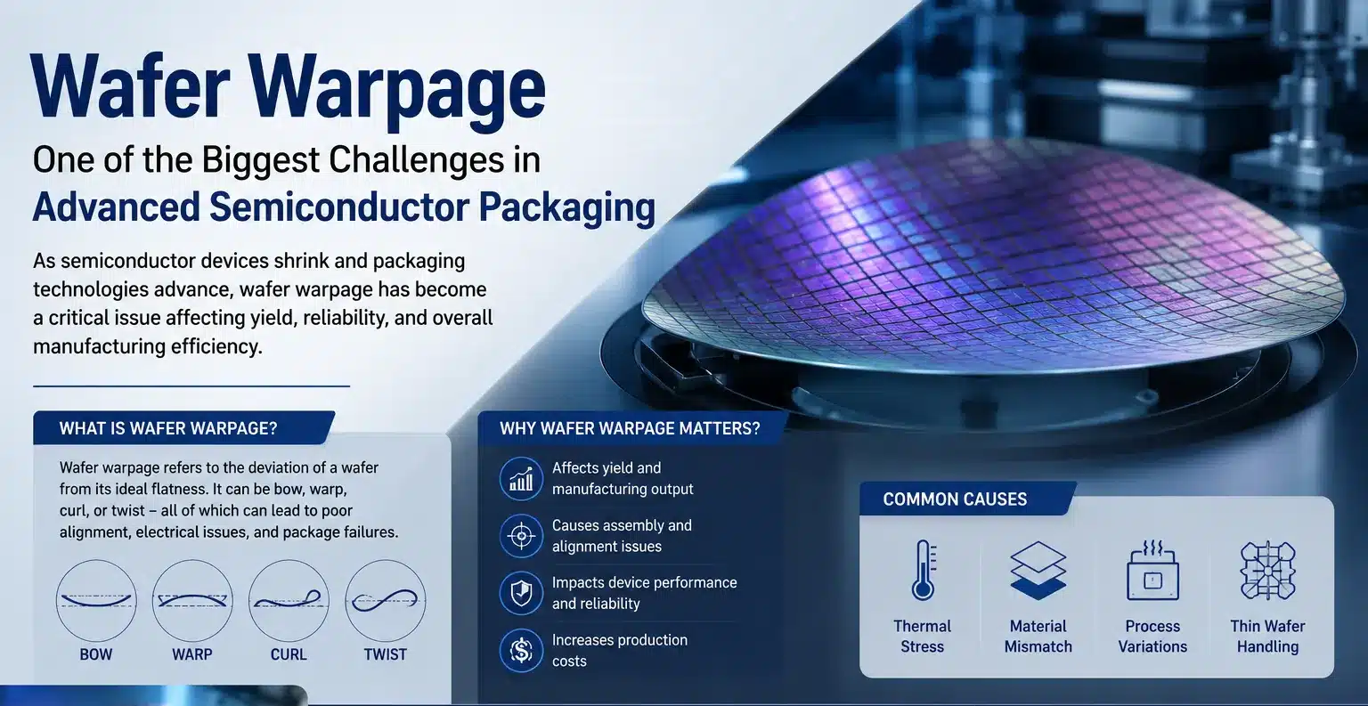
As semiconductor technology moves beyond traditional transistor scaling, advanced packaging has become the industry’s primary lever for higher performance, greater functionality, and improved power efficiency. Technologies like 2.5D integration, 3D ICs, Fan-Out Wafer Level Packaging (FOWLP), and chiplet-based architectures are redefining how next-generation chips get built. But these same innovations introduce one of the most persistent manufacturing challenges in the industry: wafer warpage.
When multiple materials with different thermal and mechanical properties are integrated into a single package, temperature changes during fabrication generate internal stresses that cause wafers to bend and deform. In high-precision manufacturing, even a few millimeters of deformation can be the difference between a high-yield production run and a costly scrap lot.
Why Wafer Warpage Matters
Wafer warpage isn’t a cosmetic defect — it’s a chain reaction that touches nearly every downstream process step. A wafer that has bowed even slightly during one process can throw off precision at every step that follows.
The most immediate consequences include:
- Alignment errors during lithography and bonding — warped wafers shift the focal plane and pattern registration, directly affecting critical dimension accuracy
- Poor wafer-to-wafer or die-to-wafer bonding — bonding processes depend on tight coplanarity; warped surfaces create voids and incomplete bonds
- Lower manufacturing yield — misalignment and bonding defects propagate into scrapped die and lower overall device yield
- Increased risk of cracking, delamination, and long-term reliability issues — stress that isn’t resolved during fabrication often resurfaces later as a field failure
Research reviewing FOWLP manufacturing has found that warpage can disrupt the manufacturing process by making it difficult for equipment to handle deformed wafers, and wafers with coplanarity issues create additional handling problems downstream In other words, warpage isn’t just a quality metric measured after the fact — it can physically interfere with equipment’s ability to process the wafer at all, from robotic handling to chuck placement.
What Causes Wafer Warpage?
Warpage in advanced packaging is driven by a combination of material, structural, and process factors that compound as packages get thinner and more heterogeneous.
Thermal expansion mismatch between materials
Every material in a package — silicon, copper, mold compound, dielectric layers — expands and contracts at a different rate as temperature changes during processing. When these coefficient-of-thermal-expansion (CTE) mismatches aren’t carefully managed, the resulting internal stress bends the wafer as it cools from process temperatures back to room temperature.
Thin wafer processing
As packages shrink and stack density increases, wafers are ground progressively thinner. Thinner wafers have dramatically less structural rigidity, making them far more susceptible to bending under the same stress levels that a standard-thickness wafer would tolerate without issue.
Redistribution Layer (RDL) stress
The RDL — the network of fine copper traces that reroutes I/O connections across a fan-out package — introduces its own stress profile. Copper distribution across the RDL that isn’t well balanced concentrates stress unevenly across the wafer surface, a factor researchers have specifically studied as a controllable warpage variable through copper volume fraction optimization.
Mold compound shrinkage during curing
In fan-out packaging, the mold compound that encapsulates and reconstitutes the wafer shrinks as it cures. That shrinkage — combined with the CTE mismatch between the mold compound and the embedded silicon die — is one of the most frequently cited root causes of warpage in FOWLP specifically, and becomes more pronounced as wafer sizes increase.
How the Industry Is Addressing Wafer Warpage
There’s no single fix for wafer warpage — it requires a combination of material science, process engineering, and increasingly, data-driven prediction working together.
Temporary wafer bonding
Attaching a rigid carrier wafer during thin-wafer processing provides mechanical support through the most warpage-prone steps, then de-bonding once the wafer is safely through those stages.
Stress compensation layers
Engineered layers designed specifically to counteract the stress introduced by other materials in the stack, effectively balancing the package from both sides rather than relying on a single low-stress material choice.
Low-stress material selection
Choosing mold compounds, dielectrics, and RDL materials with CTE values closer to silicon reduces the fundamental mismatch that drives warpage in the first place.
Optimized thermal processing
Controlling heating and cooling rates during cure and reflow steps — rather than treating them as fixed process parameters — reduces the thermal gradient stress that builds up across the wafer.
Simulation-driven design and warpage prediction
Increasingly, fabs and OSATs are using process simulation — and in more advanced deployments, machine learning models — to predict warpage before a wafer ever enters production, adjusting material selection and process parameters proactively rather than discovering warpage issues after yield data comes back. Academic reviews of FOWLP warpage now explicitly include AI/ML-based prediction methods alongside traditional theoretical and numerical modeling approaches as an emerging mitigation strategy.
Where Equipment Data and Process Visibility Fit In
Managing warpage effectively depends on tight, real-time visibility into exactly how equipment is performing at each process step — because warpage-inducing stress accumulates gradually, across cure ovens, PVD chambers, molding equipment, and thermal processing tools, not at a single isolated step.
This is where equipment connectivity and factory automation infrastructure become directly relevant to a warpage mitigation strategy, even though warpage itself is fundamentally a materials and process engineering problem. Reliable SECS/GEM and GEM300 equipment communication gives process engineers the real-time temperature, timing, and process parameter data needed to correlate specific equipment behavior with warpage outcomes measured downstream — turning warpage troubleshooting from a reactive, lot-by-lot investigation into a continuous, data-backed feedback loop.
For OSATs and advanced packaging facilities running mixed equipment fleets — often including both modern GEM300-compliant tools and older curing, molding, or thermal processing equipment that predates standard connectivity — closing that data gap is frequently the first practical step toward the kind of simulation-driven, prediction-based warpage management the industry is moving toward. Legacy equipment retrofit solutions like eInnoSys EIGEMBox exist specifically to bring that older equipment into a standardized data stream without replacing it, so warpage-relevant process data isn’t a blind spot simply because a tool is a few process generations old.
As advanced packaging continues to evolve — pushed forward by AI accelerators, high-performance computing, automotive electronics, and increasingly compact mobile devices — wafer warpage is no longer a secondary process concern that gets addressed after yield problems appear. It has become a first-order design and manufacturing constraint that has to be engineered for from the earliest stages of package design through final cure.
The path forward combines materials science, thermal process optimization, and simulation — but underneath all three, it depends on manufacturers actually having the equipment-level data needed to see where and when stress is being introduced. For fabs and OSATs working to build that visibility across a full equipment fleet, standardized equipment connectivity is the foundation everything else builds on.
What strategies have you found most effective for controlling wafer warpage in your advanced packaging processes? We’d love to hear your insights — connect with the eInnoSys team to talk through how equipment data visibility fits into your warpage mitigation strategy.


