As semiconductor manufacturing becomes increasingly automated, fabs require seamless communication between production equipment, Manufacturing Execution Systems (MES), Factory Host Systems, and business applications. This demand has made EAP Integration for Semiconductor Fabs a critical component of modern factory automation strategies.
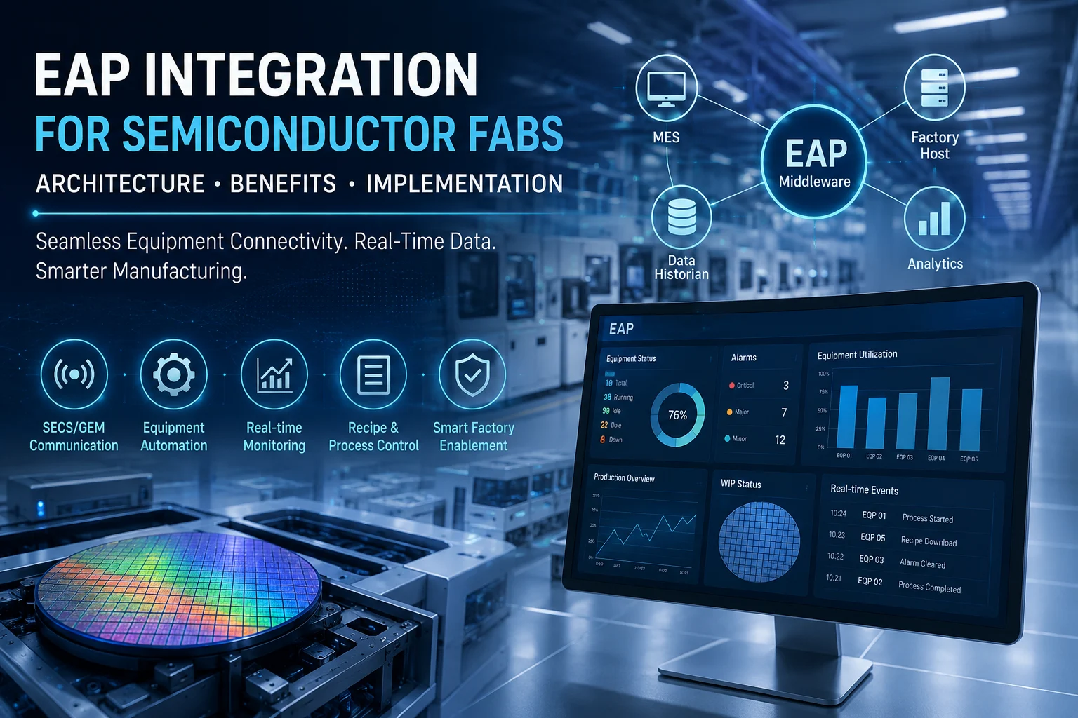
An Equipment Automation Program (EAP) acts as the intelligent middleware layer that connects semiconductor equipment with factory systems, enabling real-time data exchange, recipe management, equipment monitoring, and production control. By leveraging SECS/GEM and GEM300 standards, EAP solutions help semiconductor manufacturers improve operational efficiency, increase equipment utilization, and support Industry 4.0 initiatives.
In this article, we explore the architecture, benefits, and implementation approach for EAP Integration for Semiconductor Fabs, along with best practices for successful deployment.
What is EAP Integration for Semiconductor Fabs?
An Equipment Automation Program (EAP) serves as the communication bridge between semiconductor manufacturing equipment and factory-level applications such as MES, Scheduling Systems, Data Historians, and Yield Management Systems.
The primary goal of EAP Integration for Semiconductor Fabs is to automate data collection, equipment control, recipe verification, process tracking, and production execution while reducing manual intervention.
Typical EAP functions include:
- SECS/GEM communication management
- Equipment status monitoring
- Alarm collection and notification
- Recipe management and verification
- Wafer tracking and genealogy
- Production dispatching
- Data collection and reporting
By implementing a robust EAP Framework Semiconductor environment, fabs can achieve greater visibility and control across manufacturing operations.
EAP Architecture Design for Semiconductor Manufacturing
A well-designed EAP Architecture Design forms the foundation of successful factory automation.
Equipment Layer
This layer consists of semiconductor tools such as:
- Lithography Systems
- Etch Equipment
- CMP Tools
- Metrology Systems
- Inspection Equipment
- Deposition Systems
These tools communicate using industry-standard protocols such as SECS/GEM and GEM300.
EAP Middleware Layer
The EAP layer acts as the central integration hub responsible for:
- Data acquisition
- Equipment control
- Event processing
- Recipe validation
- Alarm management
The Equipment Automation Architecture enables centralized management of communication between hundreds or thousands of manufacturing tools.
Factory Applications Layer
This layer includes:
- MES Systems
- Scheduling Applications
- Advanced Process Control (APC)
- Yield Management Systems
- ERP Platforms
The overall Factory Automation Architecture ensures smooth information flow across all manufacturing systems.
Understanding EAP Data Flow Architecture
One of the most important aspects of EAP Integration for Semiconductor Fabs is establishing an efficient EAP Data Flow Architecture.
The typical workflow follows these steps:
- Equipment generates process data.
- SECS/GEM messages are transmitted to the EAP.
- EAP validates and processes the data.
- Information is routed to MES and factory systems.
- Production decisions are executed automatically.
- Commands are sent back to the equipment.
This architecture enables real-time visibility into equipment performance, process quality, and production status.
A properly implemented Semiconductor Integration Architecture eliminates information silos and improves manufacturing responsiveness.
Benefits of EAP Integration for Semiconductor Fabs
Improved Equipment Utilization
By automating communication and reducing manual processes, EAP Integration for Semiconductor Fabs helps maximize equipment availability and utilization.
Enhanced Production Efficiency
Automated recipe validation, dispatching, and lot tracking reduce operator errors and improve production throughput.
Real-Time Visibility
Manufacturing teams gain access to real-time equipment status, alarms, and process data for faster decision-making.
Better Quality Control
EAP systems ensure process recipes are verified before execution, minimizing the risk of incorrect production runs.
Reduced Downtime
Automated monitoring and event management help identify equipment issues early, reducing unplanned interruptions.
Support for Smart Manufacturing
Modern EAP solutions provide the digital foundation necessary for Industry 4.0 initiatives, advanced analytics, and AI-driven manufacturing optimization.
EAP Implementation Guide
A successful EAP Implementation Guide should follow a structured methodology.
Step 1: Define Business Requirements
Identify:
- Equipment types
- Factory systems
- Data collection requirements
- Production workflows
Step 2: Assess Equipment Readiness
Evaluate existing equipment communication capabilities, including:
Step 3: Design Integration Architecture
- Develop a scalable Semiconductor Integration Architecture that supports future expansion and factory growth.
Step 4: Develop EAP Software
Customized EAP Software Development may be required to support specific fab requirements, workflows, and equipment interfaces.
Step 5: Conduct Testing
Testing should include:
- Communication validation
- Data integrity verification
- Recipe management testing
- Alarm handling verification
- Production simulation
Step 6: Deployment and Training
- Successful EAP Deployment: Semiconductor projects require operator training, documentation, and ongoing support.
EAP Integration Best Practices
Organizations planning EAP Integration for Semiconductor Fabs should follow proven industry practices:
Standardize Communication Protocols
Use SEMI standards such as:
- SECS-I
- HSMS
- GEM
- GEM300
Build for Scalability
The architecture should support future equipment additions and factory expansion.
Prioritize Cybersecurity
Protect communication channels and manufacturing data through secure network architecture and access controls.
Collaborate with Experienced Partners
Working with experienced semiconductor automation providers significantly reduces project risk and accelerates implementation success.
These EAP Integration Best Practices help ensure long-term reliability and performance.
Conclusion
As semiconductor fabs continue their journey toward smart manufacturing, EAP Integration for Semiconductor Fabs has become a strategic requirement rather than an optional enhancement. A robust EAP environment enables seamless communication between equipment and factory systems, improves operational efficiency, reduces manual intervention, and supports advanced automation initiatives.
By investing in a scalable Factory Automation Project supported by strong EAP Architecture Design, effective EAP Software Development, and proven implementation methodologies, semiconductor manufacturers can achieve higher productivity, better quality control, and greater manufacturing agility.
Organizations that successfully implement EAP solutions today will be better positioned to support future Industry 4.0, AI-driven manufacturing, and next-generation semiconductor production requirements.


