
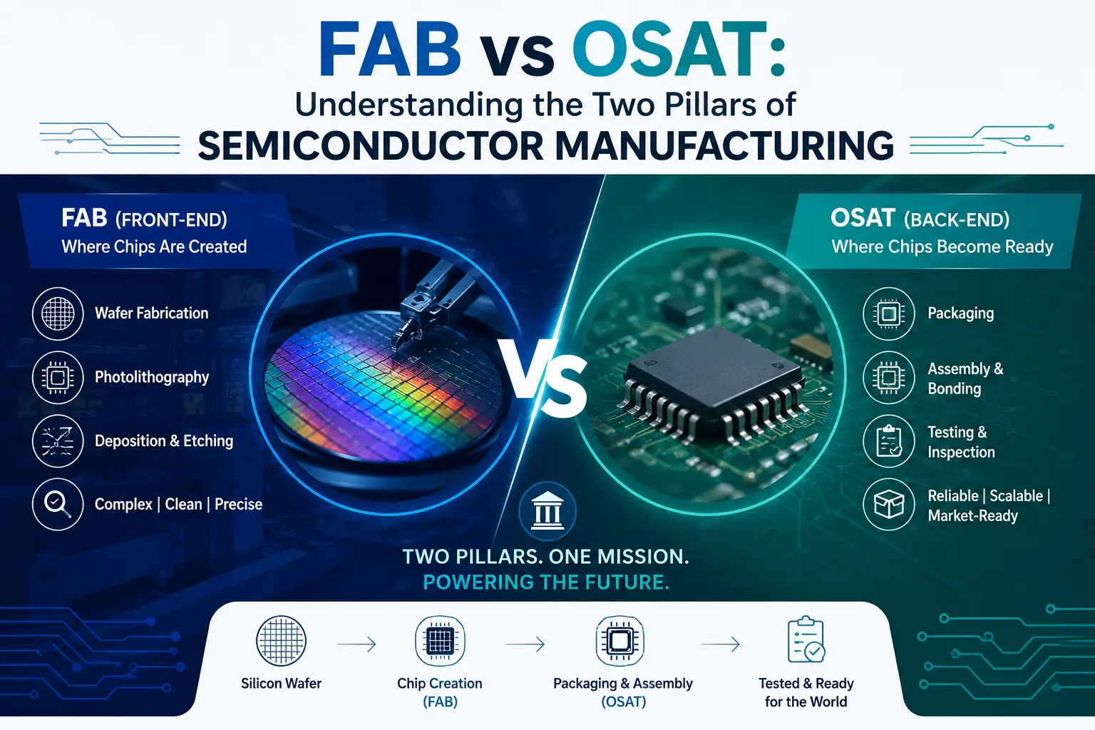
The global semiconductor industry is expanding at a pace few sectors can match, driven by AI computing, electric vehicles, 5G, and consumer electronics. Behind every chip that powers these technologies lies a two-stage manufacturing journey — one that starts in a FAB and ends at an OSAT facility. Understanding FAB vs OSAT is essential for engineers, plant managers, and technology leaders who want a clear picture of how semiconductors actually get made.
While both play indispensable roles, they operate very differently — different equipment, different cleanroom standards, and different digital transformation needs. This guide breaks down what a FAB does, what an OSAT does, how they work together, and why Industry 4.0 smart factory solutions are becoming critical to both.
What Is a Semiconductor FAB?
A semiconductor FAB (fabrication facility) is where raw silicon wafers are transformed into functional circuits. This is the front-end of semiconductor manufacturing, and it’s arguably the most capital-intensive and precision-driven process in modern industry.
Inside a FAB, wafers move through a sequence of highly controlled steps:
- Wafer preparation – cleaning and priming raw silicon wafers
- Photolithography – patterning circuit designs onto the wafer surface
- Etching – removing material to carve out circuit structures
- Ion implantation – introducing dopants to alter electrical properties
- Thin-film deposition – building up material layers
- Chemical mechanical polishing (CMP) – flattening surfaces between layers
- Wafer inspection – verifying pattern accuracy and detecting defects
FABs are operated by IDMs (Integrated Device Manufacturers) like Intel and Samsung, as well as pure-play foundries such as TSMC and GlobalFoundries. Because a single contamination event or misaligned recipe can ruin thousands of dollars of wafers, process control and yield management are the beating heart of FAB operations.
What Is an OSAT Facility?
OSAT stands for Outsourced Semiconductor Assembly and Test. This is the back-end stage of semiconductor manufacturing, where finished wafers are turned into usable, packaged chips.
Core OSAT activities include:
- Wafer dicing – cutting wafers into individual dies
- Die attach – mounting dies onto substrates or lead frames
- Wire bonding / flip-chip packaging – creating electrical connections
- Encapsulation – protecting the die with molding compound
- Final testing – verifying electrical performance
- Burn-in and reliability testing – stress-testing under real-world conditions
Many semiconductor companies choose to outsource these steps rather than build back-end capacity themselves. It reduces capital expenditure, gives access to advanced packaging expertise, and adds flexibility as product volumes and package types change. Companies like ASE Technology, Amkor, and JCET are among the world’s leading OSAT providers.
FAB vs OSAT – A Detailed Comparison
Here is your content in a clean table format:
| Aspect | FAB | OSAT |
|---|---|---|
| Manufacturing stage | Front-end | Back-end |
| Main output | Processed wafers | Packaged and tested ICs |
| Capital intensity | Very high | Moderate to high |
| Cleanroom requirement | Extremely stringent | Less stringent |
| Key technologies | Lithography, deposition, etching | Packaging, bonding, testing |
| Primary focus | Yield and process precision | Reliability and throughput |
At a glance, the difference comes down to this: a FAB builds the chip, and an OSAT makes the chip usable.
How FAB and OSAT Work Together
Semiconductor manufacturing is a relay, not a single race. A typical flow looks like this:
- Chip design is finalized by the fabless company or IDM
- Wafer fabrication happens inside the FAB
- Wafer probe testing checks individual dies while still on the wafer
- Good wafers are shipped to an OSAT facility
- Assembly and packaging convert dies into finished components
- Final electrical testing confirms performance and reliability
- Packaged chips are delivered to electronics manufacturers
FAB and OSAT are complementary business models, not competitors. A delay or quality issue at either stage ripples through the entire supply chain, which is why tighter digital coordination between the two is becoming a competitive necessity.
The Rise of Advanced Packaging
Packaging is no longer just protective housing — it’s becoming a performance lever in its own right. Trends reshaping the OSAT landscape include:
- 2.5D and 3D packaging for higher density and shorter interconnects
- Chiplets, which combine multiple smaller dies into one package
- Fan-out wafer-level packaging (FOWLP) for thinner, higher-performance devices
- High-bandwidth memory (HBM) integration for AI and HPC workloads
As chip performance increasingly depends on how it’s packaged, not just how it’s fabricated, OSAT companies are evolving from cost-driven subcontractors into strategic technology partners.
MES and Industry 4.0 in FAB Operations
Modern FABs run on data as much as they run on chemistry. Smart manufacturing capabilities that improve FAB performance include:
- Real-time production monitoring across every tool and process step
- Recipe management to ensure consistency across equipment
- Equipment connectivity through SECS/GEM and GEM300 standards
- Automated dispatching to reduce idle time and bottlenecks
- End-to-end traceability and genealogy for every wafer lot
- AI-driven fault detection and predictive maintenance
- Continuous OEE optimization
This is where Industry 4.0 smart factory solutions come in. Platforms like EINNOSYS connect FAB equipment, MES, and analytics layers so operators get real-time visibility into yield, downtime, and process drift — turning a data-heavy environment into an actionable one.
Digital Transformation in OSAT Facilities
OSAT facilities are catching up fast on the same digital maturity long associated with FABs. Key areas of transformation include:
- Managing high-mix package portfolios without losing traceability
- Collecting and analyzing test data at scale
- Automated material tracking through assembly and test lines
- Integration between testers, handlers, MES, and ERP systems
- Predictive maintenance for packaging and test equipment
- AI-based quality analytics to catch reliability issues early
The takeaway: OSAT operations now need the same level of data visibility and automation traditionally reserved for front-end FABs, especially as advanced packaging adds complexity to back-end processes.
Key Challenges in FAB and OSAT
FAB Challenges
- Multi-billion-dollar capital investment requirements
- Frequent technology node migration
- High sensitivity to yield loss
- Costly impact of equipment downtime
- Complex, tightly coupled process integration
OSAT Challenges
- Rapidly evolving package technologies
- Strict thermal and reliability requirements
- Shorter product life cycles
- Rising throughput expectations
- Managing highly diverse customer requirements
Which Model Is More Important?
This isn’t really a competition. FABs create the semiconductor devices; OSATs make them usable in real-world products. Neither can deliver value without the other. Advanced AI accelerators, automotive electronics, and high-performance computing systems all depend on innovation from both sides of the value chain simultaneously. The future of semiconductor manufacturing lies not in choosing one over the other, but in building tightly integrated digital ecosystems that connect FAB and OSAT data, quality systems, and supply chains.
FAB vs OSAT in the Indian Semiconductor Ecosystem
India’s semiconductor ambitions are accelerating, backed by government incentives aimed at building both front-end and back-end capacity domestically. Key developments shaping this ecosystem include:
- National semiconductor mission incentives supporting FAB and OSAT investments
- Strong near-term growth opportunities in packaging and testing, which require lower capital entry than FABs
- Gradual expansion of domestic wafer fabrication capabilities
- Growing importance of automation, MES, and equipment integration as new facilities come online, so they launch with Industry 4.0 maturity rather than retrofitting it later.
For India’s emerging semiconductor hubs, getting the digital infrastructure right from day one will be as important as the physical infrastructure itself.
Conclusion
At its core, the FAB vs OSAT comparison comes down to this: FAB handles front-end wafer fabrication, while OSAT manages back-end assembly, packaging, and testing. Both are essential, interdependent pillars of semiconductor manufacturing, and as chip designs grow more complex — through chiplets, advanced packaging, and AI-driven workloads — the collaboration between FAB and OSAT operations only becomes more critical.
Industry 4.0 technologies — including MES, SECS/GEM connectivity, AI analytics, predictive maintenance, and smart factory platforms — are becoming the connective tissue that ties these two environments together.
Looking to connect semiconductor equipment, improve MES visibility, enable SECS/GEM integration, and build a smarter semiconductor factory? Explore EINNOSYS Industry 4.0 Smart Factory solutions to accelerate digital transformation across FAB and OSAT operations.


